DIY USB Power Delivery Lab Bench Power Supply
Index
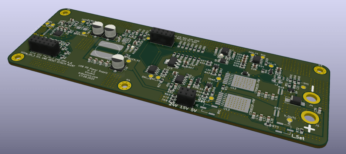
Today I want to write about the journey of designing and building my own DIY USB Power Delivery Lab Bench Power Supply. I want to address all the different steps needed to bring a project idea to life. I have to say, this project is still a work in progress, and I already found a few mistakes. Therefore you should not take my plans at the moment to build your own.
The Problem
There are a few essential tools you need when working on electronic projects. At first, you need a Multimeter. You need to be able to measure voltage and current accurately. And even though you can pay many hundreds of dollars on such a tool, you don’t have to. On Amazon, you can find many multimeters in the 20 to 50 dollar range. They definitely won’t have the latest features or have the most incredible accuracy but work well enough for nearly every hobby project you can imagine.
Another essential tool is a soldering iron. I would recommend you invest in a temperature-controlled iron with changeable tips.
My third most used tool is my Lab Bench Power supply. That’s the one I want to focus on today. Often you need to be able to inject power in your project.
The main features such a PSU should have are constant current (CC) and constant voltage (CV) mode. This means you can set a voltage and a current, and the PSU will never go above the set values. So you can, for example, set 5V and 3A to power a raspberry pi or 20mA and 5V to measure the forward voltage of a LED. And because you set the maximum current to 20 mA, you won’t even need a resistor for the LED.
My current Power supply
The Lab Powersupply (PSU) I use at the moment is called QT3005T. It is capable of a max output of 32V and 5A.

It works ok, but lately, I found out neither the current nor the voltage were accurate. While the output voltage is lower than set and shown, the output current is higher than set.
Most of the time, this doesn’t matter. The offsets are only a few hundreds of mV and a couple of mA. And a light bulb doesn’t care if you give it 12.0V or 12.2V. But a 3.3V microcontroller or sensor could get damaged if you feed it 3.5V.
I tried to recalibrate the display, but this is sadly not possible. Therefore I decided I need a new PSU. While looking at my options, I decided to design my own DIY USB Power Delivery Lab Bench Power Supply and take you along.
Design constraints
The first things you need when starting a new project are your design constraints. Here you have to decide on the basic specs. And although you can change them later, of course, you should try to stick with them
My design constraints
- Powered via USB-C PowerDelivery
- 0V – 16V
- 0A – 3A
- CC-Mode
- CV-Mode
- show regulation mode (CC or CV)
- to show the actual current
- and to show the actual voltage
- controlled via microcontroller
Research
When you decided what you want, you have to find a way to accomplish your goal. These days you can probably find someone who has written about a similar problem on the internet. A list of the links I found and my annotations can be found on the log page for this project.
Topology
So while googling, I found an article from Analog Devices about a High Performance Portable DC Bench Power Supply. The specs sounded great (0-24V and 0-3A), and it looked quite simple. Therefore I settled with this as my general topologies. It consists of a switch-mode power supply feeding a linear regulator with just a little more than the output voltage. This combines the incredible efficiency of a switching regulator with the excellent output characteristics of a linear regulator.
USB PD
With USB 3.0, the USB Power Delivery specification became popular. USB PD can deliver up to 100W via a USB-C cable. That’s the reason why many modern devices like Laptops often can be charged over USB. And a potential 20V/5A is more than enough for my requirements. So how do you get 20V on USB? Of course, you could take a microcontroller and implement the needed communication between your device and the charger by yourself. But this would be a tough and time-consuming challenge. Luckily I am not the only one with that problem, and many vendors have decided to sell ICs solely for USB PD communication. The TPS65986, FUSB302, and STUSB4500 are the ones I found to sound promising. In the end, I decided on the STUSB4500 because it doesn’t need an additional microcontroller, was available, and I found a few projects using this IC. This makes debugging, hopefully, easier.
The interface
At the moment, I haven’t decided how the interface will look like. Neither have I decided what capabilities I would like it to have. But as in my design constraint stated, I want it to be controllable via a microcontroller. This constraint was enough to start designing the power stage of this project. If that is working, I will focus on the interface.
Power supply design
The gold standard for a Lab Bench Power Supply is a linear supply. That’s because of the output characteristics. Since there is no switching supply, you have a very stable and ripple-free output and a very fast transient response. Additionally, we don’t want much output capacitance. For example, we don’t have any clue about the forward voltage of a LED. Then we could set the PSU for 20mA@10V. This means I want to have a maximum of 20mA flowing at a voltage of 10V or below. The 10V would instantly destroy the LED, but because we only supply 20mA, the LED will survive and drag the voltage down to its forward voltage at 20mA. But if a large capacitor was charged to 10V, enough energy could be stored to destroy the LED with very high currents even though we have a current limit set. That’s why I want a linear voltage regulator to control my output.
The problem with the power
But dut to the operational principles of such a regulator, the input and output currents are the same. And the voltage/power we don’t need will be converted to heat. So if we want an output of 1A@1V but have an input voltage of 20V, we would have to burn 19V@1A. That’s an input of 19W at an output of 1W. An Efficiency of about 5%. Not very good. Additionally, we have to provide a lot of cooling. And I don’t want big heat sinks and loud fans.
The solution is to feed the linear regulator just the output voltage plus the bit it needs to function correctly. Analog devices design decided on a voltage of Vout + 1.6V. When we now redo our calculation, we have an output of 1A@1V and an input of 1A@2.6V. That’s an input of 2.6W at an output of 1W. An Efficiency of 38% in a worst-case scenario. Not perfect, but way better.
A BUCK converter will supply the power to the linear regulator. By switching current through a coil and smoothing the voltage with capacitors, we can step down voltage with a very high efficiency of up to 95%.
This efficiency should be high enough that my circuit may not even require heatsinks at all.
Analog devices design intended the LT8612 as the BUCK regulator IC. But when checking Digikey, the supplier I used for my parts, I saw, this IC costs around 10€. Therefore I decided to search for another BUCK regulator. I decided on the SIC437 from VISHAY. With a cost of 3€ per chip, it is way cheaper but just as capable for my application. And the feedback circuitry needed to set the output voltage is nearly identical.
Current capabilities
The LT3081, the linear regulator, is only rated to a current of 1.5A. That’s only half of the 3A stated in the design constraints. Normally it is not a good idea to put two linear regulators in parallel. Because if their voltages are not the same, and they won’t, one will have to work way more than the other, and you need big load balancing resistors. That’s not ideal. But the LT3081 the special feature that it can be parallelized with a load balancing resistor of only 10mΩ. This resistance could even be achieved with a PCB track if needed.
The problem with zero volts
An output voltage of 0V. Sounds simple, right? Well, it’s not. Most adjustable linear regulators can’t go down to an output voltage of 0V. And even though right at the top of the LT3081s datasheet, it says “Output adjustable to 0V”, we have to work for that. To achieve such a low output voltage, there has to be a minimum output current of 4mA. For the two linear regulators, there has to be a constant current sink of 8mA a 0V. The analog device’s design uses a negative 5v supply, a resistor, and an NPN transistor connected with its base to GND.
Constant Voltage
To set the output voltage of the LT3081, you normally have to connect the set pin via a resistor to GND. The IC has an internal current source of 50uA flowing out, and the voltage over the external resistor is the voltage the regulator tries to output. Using a potentiometer, the output voltage can be set to any value just as you want for a power supply. But to control a resistor digitally with a microcontroller is not that simple. You could connect a motor to the wiper of the potentiometer. But that would be mechanically complex and big. A digital potentiometer is another option. But they are quite expensive, only very few resistor values are available, and they have a poor resolution of mostly 8 bit (256 steps). Luckily you can forcefully drive the set pin to a voltage to set the output. And generating analog voltages with a microcontroller can be done by using a DAC (Digital-Analog converter). Its output from 0V-5V is then multiplied by a factor of ~4 with an OP-Amp to get a voltage for the set pin between 0V and ~20V.
Constant current
The LT3081 has a pin for current limiting. The wanted maximum current can be set by connecting a resistor between the voltage output and the Ilim pin. Here we have the same problems with controlling a resistor digitally. Another problem is that there is no mention of controlling the current via an external voltage or current in the datasheet. Luckily I could find a thread on the EEVBlog forum. Here they were talking about a Power supply from Frex form the diyaudio forum. His design also used the LT3081. The trick is to insert a current between 0A for 0A maximum Current output and 60uA for 1.5A output per IC in the ILim pin. This could be confirmed by a small simulation using LTSpice (a free circuit simulator from analog devices. A model of the LT3081 was already included). The simulation can also be found on the Github page. How reliable this works in the real-life will be tested once the board is built.
Schematic and PCB design
The schematic design was pretty straight forward. It was mostly copying the typical application and checking the component values with the datasheet formulas. I will go over the exact schematic for the individual ICs in the future. The only parts that are not copied from the datasheets are the controls for digital control. Those are mostly copied from Frexs design. I used KiCAD for the schematic and PCB design. It is free, open-source, and has every feature you could ever want for your hobby project. Great tutorials can be found on youtube. Just as a tip, Leds and testpoints for all relevant voaltages help a ton when debugging your circuit.

Where I’m at
To be honest, there is not much I can add at the moment. The Boards are ordered from Aisler and the components on their way from Digikey. I will update this post when the Boards arrived and I had the time to get it working and tested.


6 Comments
Johannes
Again another great tutorial where you resume all your design steps. Can’t wait for the board to be finished! Have good fun along the way 🙂
Mamie Leonardo Pallaton
Helpful information. Lucky me I found your site accidentally, and I’m stunned why this twist of fate didn’t happened in advance! I bookmarked it. Mamie Leonardo Pallaton
film
I like this site very much, Its a very nice position to read and receive info . Lori Stillman Keely
Frex
Hello,
I’m happy to see that a part of my EPSUX3 design is used by others,
and furthermore in open source project, congrat !
😉
Frex
Vincent
Hi Frex,
Your design was an incredible resource while figuring out how to work with the lm3081.
Thank you very much for your work and for sharing it with the world!
Vincent
Atul Desai
I am interested in assembling a unit. I have seen your PCB can you give me one I will pay for it.
I am staying in Mumbai India Please reply.